NCBJ scientists study the structure of materials using a new microscope
2023.09.18 9:01 - Piotr Spinalski
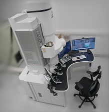 Material Research Lab and NOMATEN Centre of Excellence study and test, among other things, structural materials and their combinations, using modern, specialised analysis equipment. The laboratories’ research infrastructure now includes a recently launched transmission electron microscope.
An integral aspect of materials in nuclear applications research involves understanding radiation effects, as this knowledge is fundamental to comprehending degradation behavior. Furthermore, a thorough understanding of sample microstructure assists in accounting for irradiation effects in design and the development of new radiation-tolerant or resistant materials.
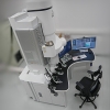
Recently, the transmission electron microscope JEM-F200 by JEOL has been installed in one of the laboratories at the NOMATEN CoE. The microscope is equipped with the Schottky-type Field Emission Gun (FEG), ensuring a highly focused, bright and stable electron beam, allowing for high-resolution imaging (up to 0.06 nm in TEM mode – lattice resolution) and precise analytical measurements. The system includes a double tilt holder for comprehensive sample observation, a straining in-situ holder for studying material deformation, a heating in-situ holder reaching temperatures up to 1000°C, and a tomography holder for three-dimensional imaging.
The primary application of TEM at NOMATEN involves examining radiation-induced changes in materials at the nanoscale, such as dislocation lines, planar defects like stacking faults, and volume defects such as voids, bubbles and precipitates. TEM also aids in determining the crystallographic alignment of defects, phases, and other microstructural features in the materials.
The use of TEM can contribute to the understanding of many scientific problems that are under intense discussion in the materials science community. They can be generally described as the association of microstructure transformations with changes in functional properties, e.g. degradation under ionizing radiation.
„NOMATEN’s new TEM equipped with two EDS detectors allows for qualitative chemical composition analysis through point analysis, line scans, or mapping of chemical composition distribution at resolution of several nanometers” – describes Iwona Jóźwik, PhD, leader of the Materials Characterization Research Group at NOMATEN CoE. ”Moreover, TEM permits the 3D reconstruction of sample volumes within complex materials, facilitating the study of precipitates in matrices, nanoparticle distribution, dislocations and grain boundaries. Understanding these defects’ distribution is crucial for comprehending changes in the mechanical properties of materials, embrittlement phenomena, and material failure.”
In addition to studying the microstructure of materials under irradiation, the laboratory will also facilitate in-situ tensile testing experiments, which will offer valuable insights into the deformation mechanisms of materials. In such experiments materials are subjected to controlled mechanical loads while simultaneously observing dynamic modifications of their microstructure using advanced electron microscopy techniques. This makes possible to investigate the evolution of defects and the mechanisms through which they contribute to material deformation and failure. Comparing TEM in-situ deformation results with the data obtained using other devices at NOMATEN laboratories, such as a tensile machine for miniaturized samples and a nanoindentation device, will help to design materials with optimal mechanical properties. Moreover, the investigation of changes in sample microstructure subjected to high temperature, coupled with the results from other characterization devices at NOMATEN laboratories such as high-temperature in-situ X-ray diffraction (HT-XRD) or differential scanning calorimetry (DSC) will bring a better understanding of the behavior of materials at high temperature, which is crucial for many industrial applications.
Furthermore, apart from studying radiation-induced damage in materials, the new microscope will also play a crucial role in investigating corrosion phenomena in protective coatings for applications in nuclear engineering. Protective coatings are of paramount importance in preventing the corrosion and degradation of structural materials in nuclear power plants and other nuclear applications. However, these coatings are susceptible to various environmental and operational factors that can lead to their gradual degradation, resulting in a loss of protective functionality and potentially compromising the safety and reliability of the underlying structure. The new instrument will enable the study of the microstructure and chemical composition of protective coatings at the atomic scale, providing valuable insights into the mechanisms of corrosion and degradation. Through the utilization of advanced electron microscopy techniques, researchers can observe the behavior of coatings and their interaction with the underlying substrate.
The microscopy laboratory at NOMATEN CoE is equipped with a comprehensive range of systems for the analysis and characterization of advanced materials. Various devices at NOMATEN laboratories enable sample preparation using the optimal technique (ion milling, electrolytic thinning) for specific type of material. This enables the efficient execution of characterization and research studies on-site, eliminating the need to outsource investigations. „Our workflow for structural characterization is seamlessly integrated within a single laboratory, facilitating sample preparation and analysis in the same building” – adds Iwona Jóźwik. „This arrangement minimizes the time gap between sample preparation and subsequent analysis in TEM. As a result, TEM becomes an integral component of our electron microscopy laboratory, enabling robust structural studies to be conducted within a relatively short timeframe. This significantly enhances the capabilities of the research carried out at NOMATEN CoE.” Prof. Mikko Alava, the director of the NOMATEN Centre of Excellence summarizes: „I am happy to see the arrival of this very modern piece of equipment. It completes the circle of modern materials science research at NOMATEN. I would like to thank the team that has realized this, and also the Foundation for Polish Science for the resources”.
The purchase of the JEOL JEM-F200 was financed by the European Union Horizon 2020 research and innovation program under Grant Agreement No. 857470 and from the European Regional Development Fund via Foundation for Polish Science International Research Agenda PLUS program Grant No. MAB PLUS/2018/8.
Additional information:
The principle of transmission electron microscopy (TEM) is transmitting high energy electron beam through the thin (approx. 70 nm) specimen. Images obtained this way are 2D projection of the whole volume of beam-specimen interactions. Thanks to a very short wavelength (approx. 0.002 nm for 200 kV microscopes), it is possible to detect various microstructural features like dislocations, grain boundaries, precipitates and link them with crystallographic data.
Imaging possibilities of TEM include several techniques which are dedicated for visualizing a variety of microstructural features. The most common mode is bright field which can be used as a daily routine for studying grains and dislocations. Another technique, known as dark field, allows to visualize a particular type of defect, phase or grain while keeping the rest invisible. This is particularly useful when concerning distribution of defects of interest. On the other hand, the diffraction technique allows for the determination of crystal structure of the observed objects within the materials allowing for their phase identification.
Analytical possibilities of TEM are linked with the precise control over the movement of the electron beam focused to a point. This mode is called scanning TEM (STEM) and in combination with energy dispersive X-ray spectrometry (EDS) enables analysis of chemical composition of objects with sizes measured in single nanometers, or studying distribution of elements within the field of view. Additionally, high angle annular detector allows imaging of specimen with so-called Z-contrast (related to atomic number) which is useful for studying multi-phase materials or atomic arrangements within phases.
Modern TEMs are frequently equipped with electron tomography devices which make possible to determine 3D distribution of objects within the specimen. This is modern branch of electron microscopy developing by many laboratories around the world.


